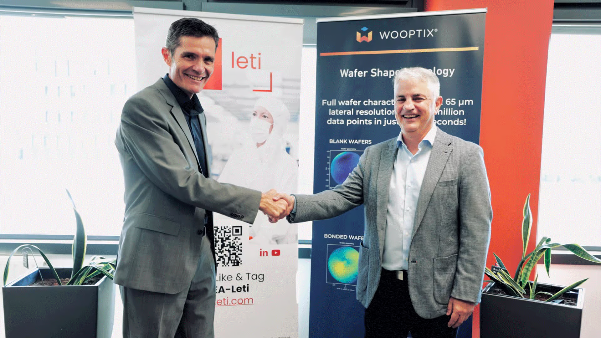
Wooptix, a Spanish semiconductor metrology company and member of the EIC Scaling Club’s Next-Gen Computing group, has installed its first production Phemet system at CEA-Leti’s research institute in Grenoble, France.
The deployment marks an important step in Wooptix’s move towards high-volume semiconductor manufacturing. Installed at CEA-Leti on 4 May 2026, Phemet will operate in the organisation’s industrial cleanroom, supporting joint work on wafer-scale process analysis, nanotopography and metrology for advanced semiconductor packaging.
Moving semiconductor metrology into production
Semiconductor manufacturers depend on precise measurements throughout production. As chips become smaller, more powerful and more complex, minor changes in a wafer’s shape or surface can affect manufacturing accuracy, device performance and production yield.
Wooptix developed Phemet to measure the shape, nanotopography and roughness of an entire 300 mm silicon wafer in a single capture. The automated system collects millions of data points and provides sub-nanometre height resolution, supporting fast in-line measurement during manufacturing.
The technology can examine blank, patterned and bonded wafers. It can also measure bow, warpage and other parameters that help engineers identify process variations and trace the causes of defects.
This first production deployment will allow Wooptix to test and refine the system in conditions that closely reflect industrial semiconductor manufacturing.
Supporting more advanced chip architectures
Demand for more accurate process control is growing as the semiconductor industry adopts smaller features, three-dimensional integration and advanced packaging methods.
These technologies place several components into increasingly complex structures. Manufacturers therefore need detailed information about the entire wafer, including small variations that may influence alignment, bonding and the performance of the finished device.
Phemet uses Wooptix’s proprietary wavefront phase imaging technology. Originally derived from adaptive optics research, the method analyses how light travels across a wafer and uses this information to construct a detailed map of its shape and surface.
By capturing the full wafer in a single image, the system is designed to combine measurement speed with high resolution. Its data can also support automated process-control methods, helping manufacturers respond to variations earlier in production.
Validating the technology in an industrial environment
The collaboration with CEA-Leti gives Wooptix access to an advanced research environment in which new semiconductor processes can be developed and evaluated.
Wooptix will use the installation to build evidence around practical process-development challenges and investigate further applications for its technology. The work will focus partly on advanced packaging, where accurate wafer-shape measurements are increasingly important for processes such as hybrid bonding and three-dimensional integration.
José Manuel Ramos, CEO of Wooptix, described the installation as a necessary step in the company’s roadmap towards applications in high-volume semiconductor manufacturing. He also highlighted the opportunity to validate Phemet alongside leading industry and research organisations in Grenoble.
CEA-Leti will evaluate the capabilities of the fully automated platform and explore how it can support a range of industrial-scale applications.
Strengthening Europe's semiconductor capabilities
The installation comes as Europe works to strengthen its position across the semiconductor value chain. Advanced metrology is an essential part of this effort because manufacturers need accurate and timely measurements to improve production processes, increase yield and develop new generations of chips.
Wooptix has offices in Tenerife, Madrid and Grenoble and is deploying its measurement solutions across Europe, Asia and North America. Its technology originated in research into adaptive optics for astronomy and has since been developed for semiconductor manufacturing.
About the EIC Scaling Club
The EIC Scaling Club is a curated community where 120+ European deep tech scale-ups with the potential to build world-class businesses and solve major global challenges come together with investors, corporate innovators and other industry stakeholders to spur growth.
The top 120+ European deep tech companies will be carefully selected from a pool of high-growth scale-ups that have benefitted from EIC financial schemes, other European and national innovation programmes, and beyond.
The EIC Scaling Club is an EIC-funded initiative run in partnership by Tech Tour, Bpifrance (EuroQuity), Hello Tomorrow, Tech.eu (Webrazzi), EurA and IESE Business School.
Subscribe to our newsletter here to stay up-to-date!